| delorie.com/pcb/lab/ | search |
Click on any thumbnail to see the full-size picture
|
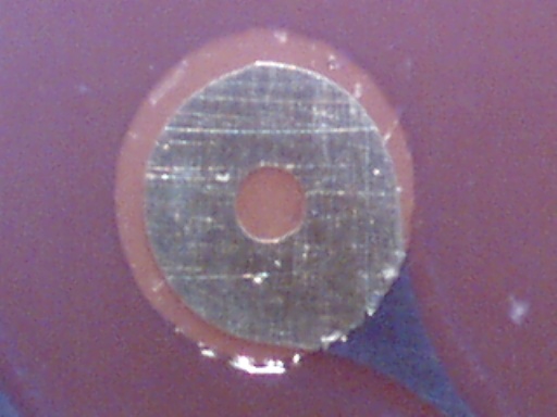
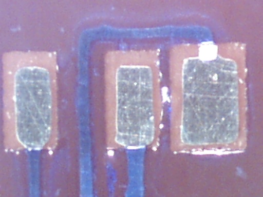
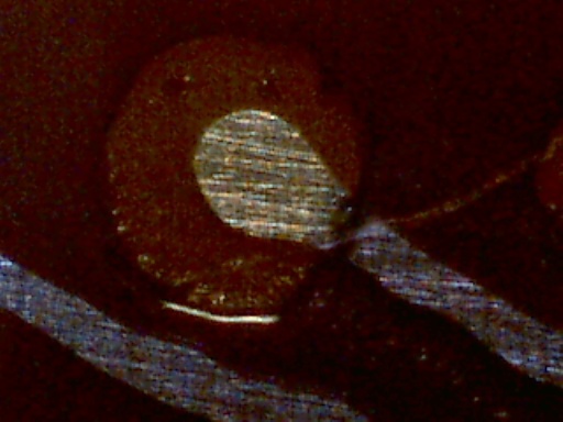
| 60x, 60x, 200x photos of Riston film used as solder mask. Now sure how well it will hold up to soldering, though. The first image is a 60 mil pad, the second is a pair of 0603 parts, the third is a BGA pad with 5 mil traces. |
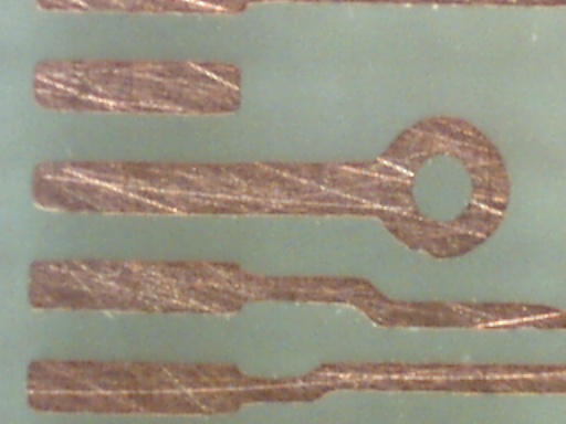
 | After etch, close-ups (200x). Note the expected undercutting, which resulted in traces just the right size. I "bloat" my films by 1.25 mil per edge. |
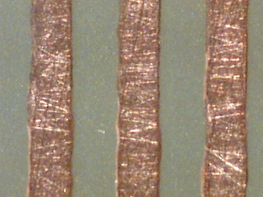
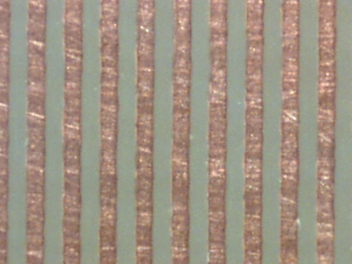
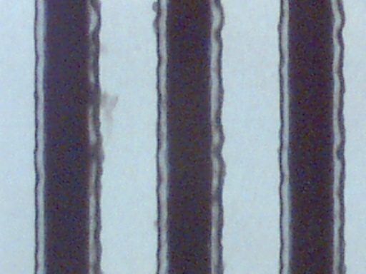
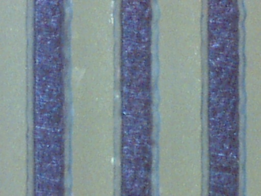
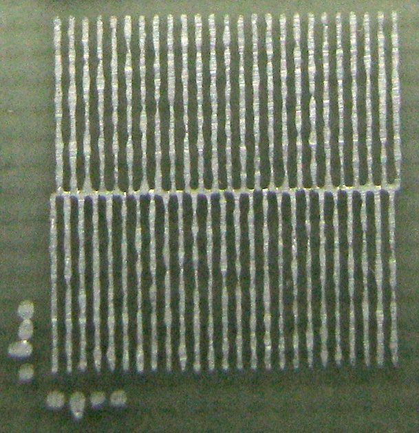
 | These traces are all 6 mil on 12.5 mil centers, or about 6/6 rules (technically, 6.25/6.25 rules). Left to right: 200x front-lit, 60x front-lit, 60x back-lit. |
 | Close-up of an 0.5mm TQFP footprint and a via. |
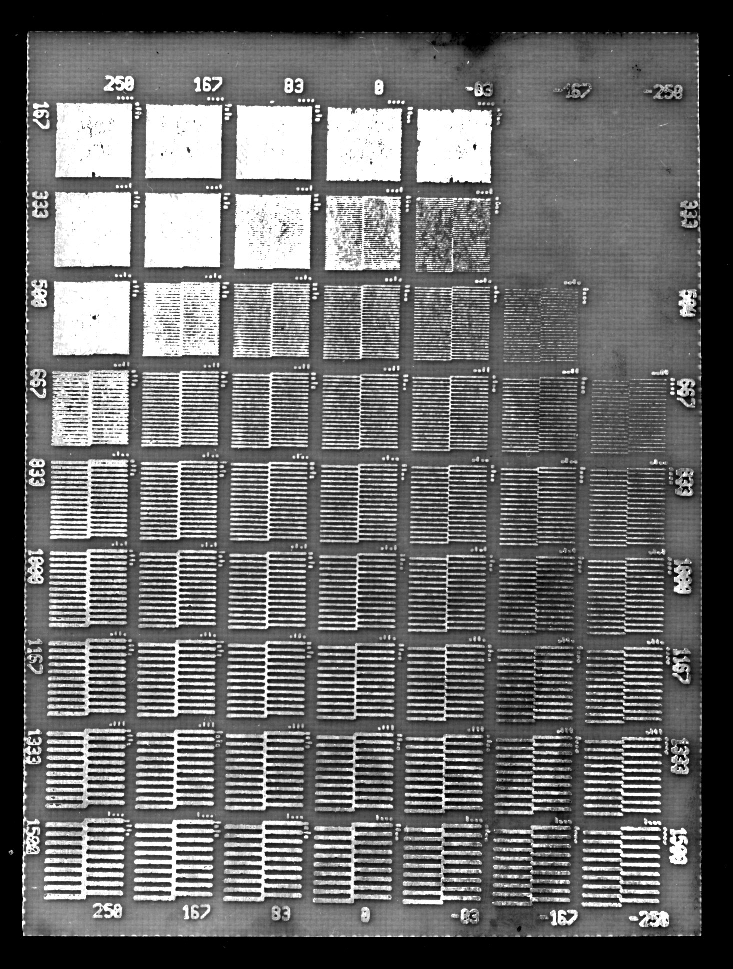
 | 5/5 rules, with traces shrunk 0.83 mil (half a pixel) per edge (i.e. 3.33/6.67 rules). |
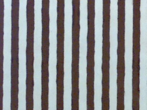
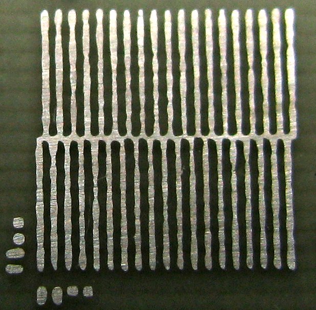 | 6.67/6.67 rules, no adjustment. |

| webmaster | delorie software privacy |
| Copyright © 2009 | Updated Dec 2009 |