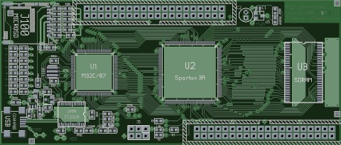
Image of board, actual size. U1=M32C, U2=Spartan 3A, U3=SDRAM

Sample Verilog simulation - click for larger view
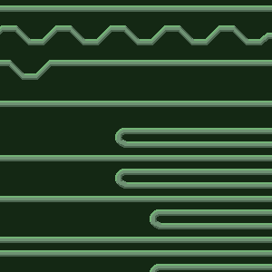
closeup of serpentines
| delorie.com/electronics/sdram/ | search |
The purpose of this project is to create a simple interface between an MCU that doesn't support DRAM, and a standard single-rate SDRAM chip. This allows small MCUs that happen to have a large memory space, to access more storage than they normally have, without having to spend lots of money and board space on static ram.
The project consists of two parts: First, the hardware. In this case, we're interfacing a Renesas M32C/87 16-bit MCU with a 16Mb external address space (minus some reserved areas) with an 8Mb or 16Mb Micron SDRAM chip. The interface is a Spartan 3A FPGA, which happens to come in a TQFP package for easy home soldering. The test board is a four-layer board because it vastly simplifies the power system, and I can make them at home as long as they're not too complex. There are also two headers for my logic analyzer; one on the MCU side and one on the FPGA side. The main signals are on the top; the bottom has the header and programming signals.
The second part is the FPGA code. We need to interface an "old school" MCU bus (address, data, read/write signals, chip select, and ready) to a modern SDRAM (address, dq, ras, cas, clock, etc). For simplicity, the board layout does a 1-to-1 mapping between the fpga pins and the chips it connects to; that allows for design changes in software rather than having to hack the board. The current design does no caching at all; each access involves a row activation, single byte transfer, and precharge. It can do writes with zero wait states (1+1 cycle) at 32MHz, and reads with 1 wait state. Note that the implementation depends on the MCU having a "ready" input so that the fpga can tell it when it's data is ready. That way, if the ram needs to be refreshed, the fpga can take time to do so.
The files below are ongoing works-in-progress. To run the verilog tests, you'll need to download the verilog code for the sdram chip (mt48lc8m16a2.v) from Micron's site.
|
|
|
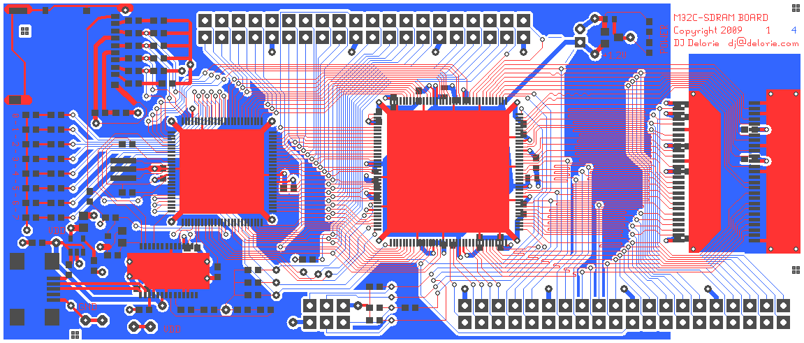
Top (red) and bottom (blue) routing layers shown 2.4X actual size.
Internal layers are GND (near top) and +3.3V (near bottom)
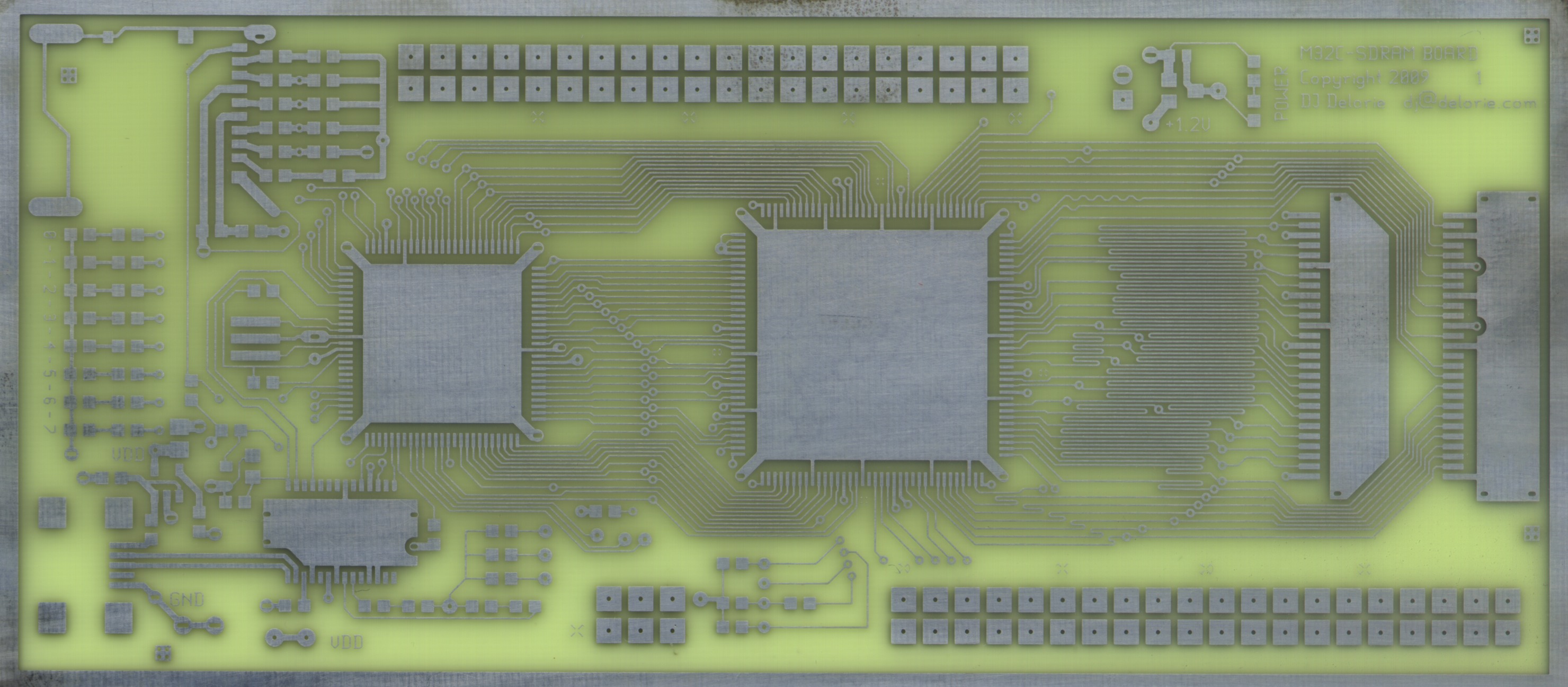
Etched top layer, 150 dpi. Click for 600 dpi version (2960x1296 pixels).
| webmaster | delorie software privacy |
| Copyright © 2010 | Updated Aug 2010 |